

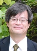
Hiroshi Amano joined Prof. late Isamu Akasaki & apos group in 1982 as an undergraduate student. After graduation, he has continued to do world-leading research on the growth, characterization and device applications of III –N semiconductors. Amano has led his own world-class research group since 1992 and in 2010, he has moved to Nagoya University. As the director of Center for Integrated Research of Future Electronics, he continues to lead the world in the creation of high-performance DUV LEDs, laser diodes, and high-power/high-frequency devices. In 2019, his group succeeded the world’s shortest wavelength laser diode emitting 271.8 nm by AlGaN-based III–N semiconductors. He shared the Nobel Prize in Physics 2014 with Prof. late Isamu Akasaki and Prof. Shuji Nakamura "For the invention of efficient blue light-emitting diodes which has enabled bright and energy-saving white light sources".

Stacia Keller received her Diploma and PhD in Chemistry from the University of Leipzig. After pursuing research in the field of conventional III-V semiconductors she joined the ECE Department at UC Santa Barbara in 1994, the beginning of her activities in the field of group-III nitrides, including their MOCVD growth, characterization, and application for electronic and optoelectronic devices. She co-advised 28 PhD students, has over 500 publications, and holds 29 U.S. patents. She received the Prize of the German Association for Crystal Growth for “Excellence in Crystal Growth of Group-III Nitrides” (2020).

Matteo Meneghini is currently Associate Professor at the University of Padova. His main research topics are the characterization, modelling and degradation of compound semiconductor devices for electronics and optoelectronics. He has given a significant contribution especially on GaN-based LEDs and lasers, GaN-based RF and power transistors, silicon carbide FETs, gallium oxide and related devices, InGaAs/InAs-based laser diodes for silicon photonics, thin-film solar cells. In these fields he has co-authored more than 450 journal and conference papers, and given invited and tutorial talks at several conferences, including IEEE-IEDM, IEEE-IRPS, IWN, ICNS, Photonics West. He is/has been in the technical committee of several relevant conferences in the field of electronics (IEEE-IEDM, IEEE-IRPS, ESREF, IWN, ESSDERC, Photonics West) and sub-committee chair for IEEE-IRPS and ESREF. He is currently editor of the IEEE-Transactions of Electron Devices, and associate editor of the IET Journal Electronics Letters. He has collaborated and/or co-published with several industries and universities active in the field of wide bandgap electronics and optoelectronics, also in the framework of international research projects. During his career, he has received several paper awards, including Best Paper Award at ESREF 2009, Best Paper Award at ESREF 2012, Best Paper Award at IWN 2012, Best paper Award at 45th Annual meeting of Gruppo Italiano di Elettronica (GE), 2013, Best paper Award at ESSDERC 2013, Best Poster Paper Award at 2014 International Reliability Physics Symposium (IEEE-IRPS 2014), Best Paper Award at ESREF 2015, Best Student Paper award at IEEE International Reliability Physics Symposium – IRPS 2018, Poster Prize at 16th International Symposium on the Science and Technology of Lighting LS16, 17th – 22nd June 2018, Sheffield, UK, Best Paper Award at 29th European Symposium on Reliability of Electron Devices, Failure Physics and Analysis ESREF 2018, Best Student Paper award IEEE International Reliability Physics Symposium – IRPS 2019, March 31 - April 4, Monterey, California, Best Paper award 30th European Symposium on Reliability of Electron Devices, Failure Physics and Analysis (ESREF 2019).

Herbert Pairitsch is Director Technology & Innovation at Infineon Technologies Austria AG, one of the leading European companies for semiconductor based power electronics. He recived a Master degree in electrical engineering from Graz University of Technology. From 1998 to 2014 Herbert Pairitsch headed of various departments in production and R&D. Since then, he held the divisional responsibility for research funding at Power & Sensor Systems (PSS), including coordination of national and international cooperative research projects in the context of energy-efficient electronics.

Euijoon Yoon received his BS (1983) and MS (1985) from Seoul National University, Korea, and PhD from MIT, USA (1990) in Electronic Materials. After Postdoctoral Member of Technical Staff at AT&T Bell Laboratories, Murray Hill, NJ, USA, he joined the Department of Materials Science and Engineering, SNU, Korea in 1992. He worked for the Office of Strategic R&D Planning, Ministry of Trade, Industry, and Energy, Korea as Managing Director from 2013 to 2017. As Dean for Research Affairs and Director of SNU R&DB Foundation, SNU, from 2019 to 2021, he worked for SNU in the field of research administration, technology transfer, and startup acceleration. He is the inventor of sapphire nano-membrane technology and is interested in the sapphire nano-membranes for discrete micro-LED for affordable large-area display fabrication. In 2020 he became Founding President of Korea Institute of Energy Technology (KENTECH), where he focuses on the undergraduate education reform in favor of inquiry-based learning and the innovative graduate research in energy sectors such as AI for energy; energy materials and devices; grid modernization; hydrogen energy; and environmental, climate technology; and nuclear fusion to cope with carbon neutrality in 2050. He is a member of the National Academy of Engineering of Korea.

Huili Grace Xing is currently the William L. Quackenbush Professor of Electrical and Computer Engineering, Materials Science and Engineering at Cornell University, having served as the Associate Dean for Research & Graduate Studies of the College of Engineering.
(She has delivered 200+ invited talks and seminar, and has authored/co-authored 300+ journal papers including Nature journals, Physical Review Letters, Applied Physics Letters, Electron Device Letters, and 120+ conference proceeding publications in IEDM, ISPSD etc. Her h-index is 70.)
She is a recipient of the AFOSR Young Investigator Award, NSF CAREER Award, ISCS Young Scientist Award, and the Intel Outstanding Researcher Award. She is a fellow of APS, IEEE & AAAS.
Tutorials

GaN technology today has developed into a mature technology for numerous applications in solid state lighting, high frequency and power electronics. Beyond that GaN optoelectronics is moving more and more into the field of photonic integration, aiming at many new and innovative applications in nanometrology and quantum technology. E.g., micro-LED arrays, being the core technology for future augmented reality and visualization, will in addition play an important role as point light sources for optical excitation in communications, imaging, and sensing. This explosion of applications is driven by two main directions: the ability to produce very small GaN light emitters, like microLEDs and nanoLEDs, with high efficiency and across large areas, in combination with the possibility to merge optoelectronic-grade GaN microLEDs with silicon microelectronics in a fully hybrid approach. Here, a particular focus will be put on applications in nanometrology, where microLEDs and nanoLEDs can be used for various sensing applications, possibly even for superresolution microscopy on a chip.

Point defects and impurities affect or even completely determine physical and chemical properties of semiconductors. Characterization of point defects based on experimental techniques alone is often inconclusive. In such cases, the combination of experiment and theory is crucial to gain understanding of the system studied. In this tutorial, I will explain how and when such comparison provides new understanding of the defect physics [1]. I will focus on processes that can be analyzed or understood in terms of configuration coordinate diagrams of defects in their different charge states. These processes include light absorption, luminescence, and nonradiative capture of charge carriers.
[1] A. Alkauskas, M. D. McCluskey, and C. G. Van de Walle, J. Appl. Phys. 119, 181101 (2016).